[Update]
I spent the day reading the SD Assoc "Physical Layer Simplified Spec v8", and then decoded what was on the SPI bus.
I was curious to understand what was going on and the low level commands.
It starts off with a slow SPI CLK of 280 Khz, then does a card reset, and checks and sets the SD cards voltages.
Then the clock frequency switches to a higher freq (in my case to 2.2xx Mhz) followed by the set up and data transfer.
(I still need to decode that section)
Here is what happens with the unmodified example code:
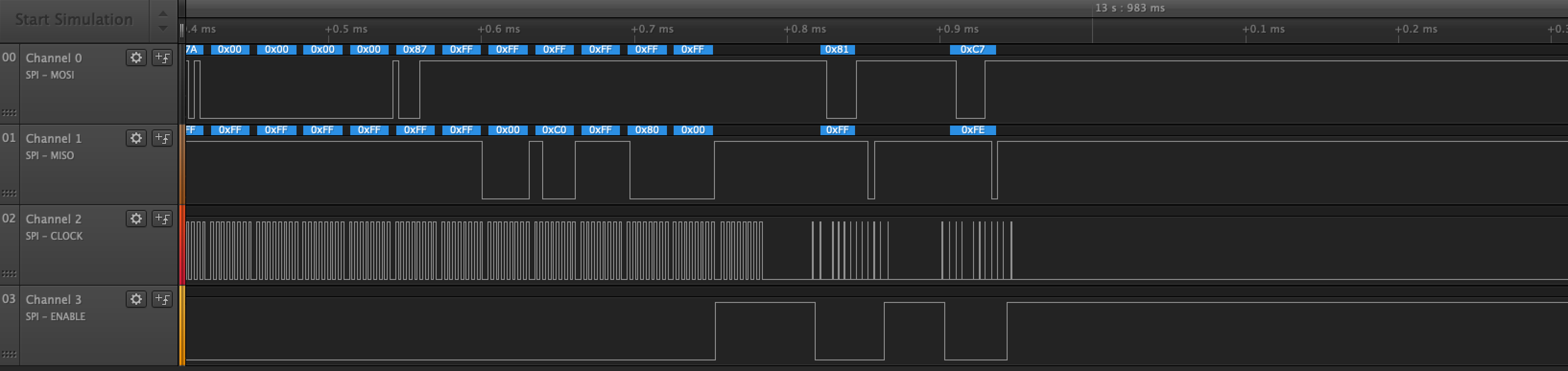
- SdFat+STM32F1_SD_fail_point.png (79.77 KiB) Viewed 1872 times
As you can see, the SPI clock stops.
Here is the CLK frequency transition point with the fix:
Code: Select all
if (!SD.begin(SD_CS_PIN, SD_SCK_MHZ(4) )) {
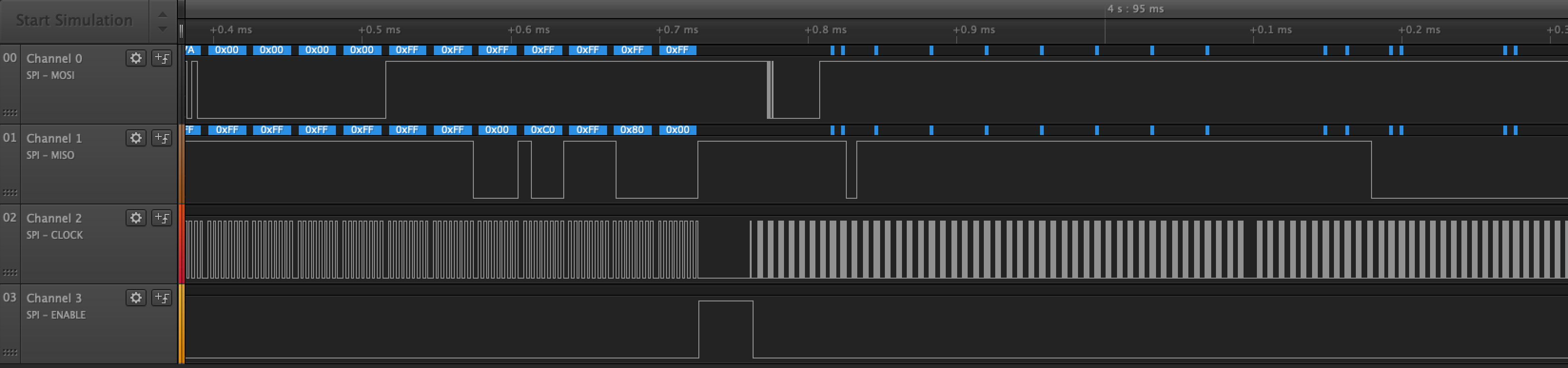
- SD+STM32F1_SD_non-fail_point.png (78.26 KiB) Viewed 1872 times
It seems like the STM32F1 couldn't switch to the higher SPI CLK frequency. -OR- it detected an error and quit.
I will test this on a few new boards... I am curious to see if I have a weak/bad one

